Dr. Murat Uzam, Academic and Technical Author, Turkey
This column is dedicated to a project involving thirteen analogue input modules and seven analogue output modules for a 5V microcontroller through its ADC and DAC channels.
In columns two to four, we discussed 0-5V analogue input modules 1 to 5. These modules accept DC input voltages from 0V to 6.26V, 12V and 24V, requiring different DC power supplies.
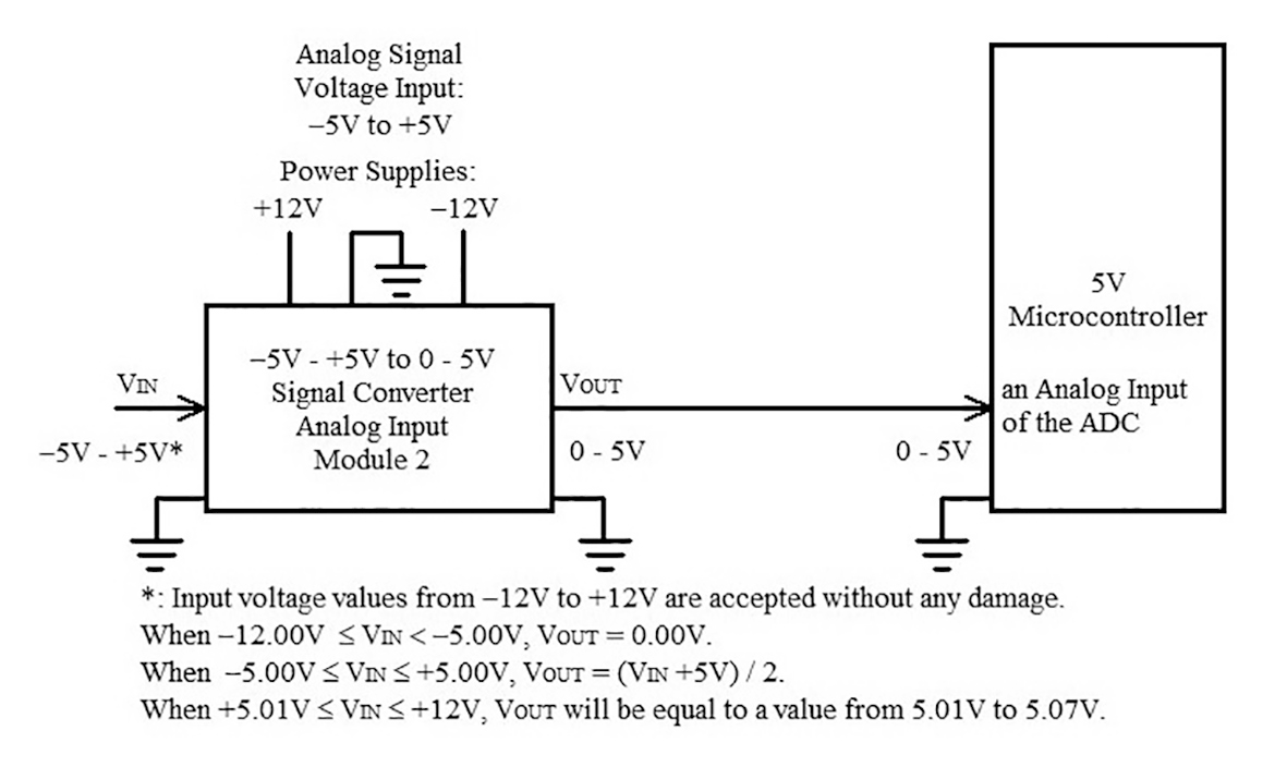
In the last column, we analysed a 0-10V to 0-5V signal converter’s analogue input modules 1 and 2. These modules accept DC input voltages from 0V to 24V and require 6.26V, 12V and 12V DC power supplies, respectively. This month, we will focus on the eighth and nineth analogue input modules, or analogue input modules 1 of a 2–5V to 5V to 0-5V signal converter. The –5V to ±5V to 0-5V signal converter input module 1 (and then respectively 2) can accept DC input voltages from –12V to 12V, and requires four DC power supplies: 5V, 6.26V, –12V and 12V, i.e. only two DC power supplies: –12V and 12V.
Analogue Input Module 1
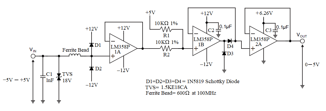
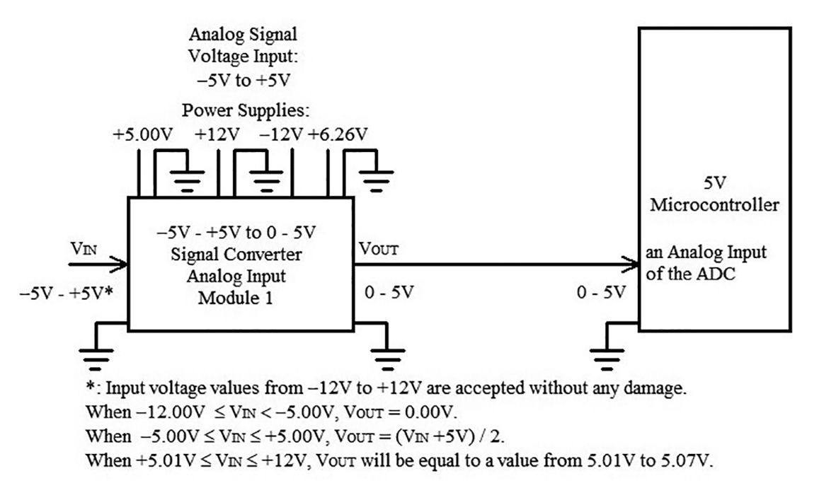
Figure 1 shows the diagram of module 1 of the -5V to 5V to 0-5V signal converter, with Figure 2 showing its connections to an analogue input of a 5V microcontroller. In this design we assumed that the input voltage range, VIN, is -12V to 12V. When -12V £ VIN < -5V, VOUT = 0V. When -5V £ VIN £ 5V, VOUT = (VIN + 5V)/2. When +5.01V £ VIN £ 12V, VOUT will be equal to a value from 5.01V to 5.07V, due to the electrical properties of the LM358P-2A used.
VIN < -5V, VOUT = 0V. When -5V ≤ VIN ≤ 5V, VOUT = (VIN + 5V)/2. When +5.01V ≤ VIN ≤ 12V, VOUT will be equal to a value from 5.01V to 5.07V, due to the electrical properties of the LM358P-2A used.
The relationship between VOUT and VIN is shown in Figure 3. It can be seen that input voltages to +12V are accepted without any damage to the circuit, and are output as a value from 5.01V to 5.07V.
This design is used to level-shift the bipolar -5V to 5V analogue voltage signal to provide a unipolar 0-5V analogue input signal.
When -5V ≤ VIN ≤ 5V, this circuit acts as a non-inverting summing amplifier with the transfer function:

Since R1 = R2:
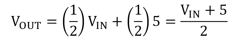
It performs analogue summation between VIN and 5V with gain of 1.
The analogue voltage input signal VIN can be subjected to electric surge or electrostatic discharge on the external terminal connections. The TVS (transient voltage suppressor) shown in the circuit provides highly effective protection against such discharges. A ferrite bead is connected in series with the input path to add isolation and decoupling from high-frequency transient noise.
External Schottky diodes generally protect the operational amplifier. Even when internal ESD protection diodes are provided, the use of external diodes lower noise and offset errors. Dual series Schottky barrier diodes D1 and D2 divert any overcurrent to the positive or negative power supply. The operational amplifier LM358P-1A, with bipolar supply voltages, provides a high input impedance and is connected as a buffer amplifier (voltage follower). +5V and R1, VIN and R2, and LM358P-1B act as a non-inverting summing amplifier. Diodes D3 and D4 make sure that when -12V ≤ VIN < -5V, VOUT = 0V. The operational amplifier LM358P-2A, with a 6.26V supply, acts as a voltage limiter and is connected as a buffer amplifier (voltage follower). VOUT is obtained from the output of the LM358P-2A.
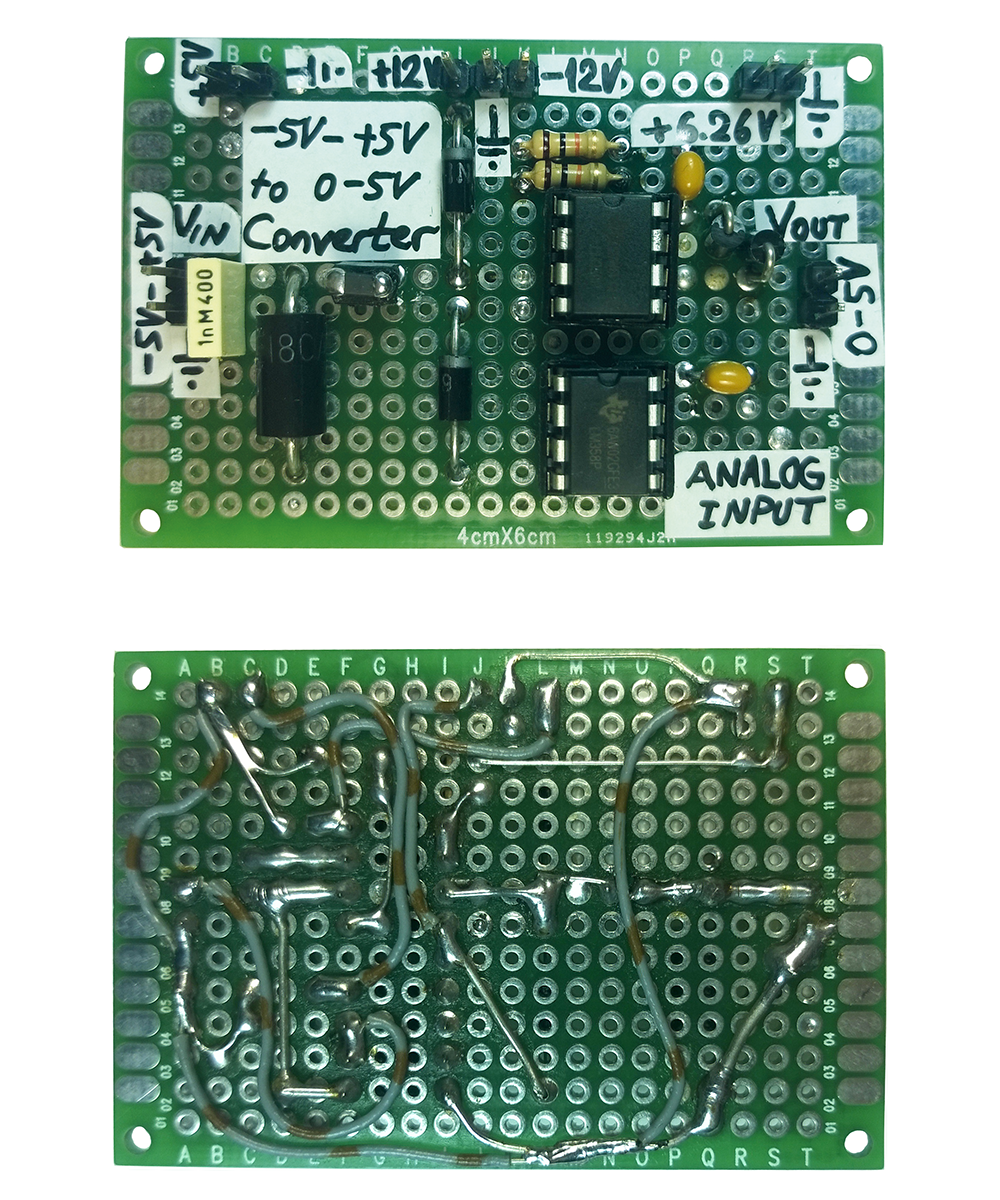
Table 1 shows some example input and output voltage values for the analogue input module 1 of the -5V to +5V to 0-5V signal converter. The top and bottom of its prototype circuit board are shown in Figure 4.
One important implementation tip for proper operation is to ensure R1 = R2 and +5V = +5V.

| VIN(V) | VOUT(V) |
| +12.00 | 5.0X |
| .. | 5.0X |
| +10.00 | 5.0X |
| .. | 5.0X |
| +5.00 | 5.00 |
| .. | .. |
| +4.00 | 4.50 |
| .. | .. |
| +3.00 | 4.00 |
| .. | .. |
| +2.50 | 3.75 |
| .. | .. |
| +2.00 | 3.50 |
| .. | .. |
| +1.00 | 3.00 |
| .. | .. |
| 0.00 | 2.50 |
| .. | .. |
| -1.00 | 2.00 |
| .. | .. |
| -2.00 | 1.50 |
| .. | .. |
| -2.50 | 1.25 |
| .. | .. |
| -3.00 | 1.00 |
| .. | .. |
| -4.00 | 0.50 |
| .. | .. |
| -5.00 | 0.00 |
| .. | .. |
| -10.00 | 0.00 |
| .. | .. |
| -12.00 | 0.00 |
Table 1. Some example input and output voltage values of analogue input module 1 of the -5V to 5V to 0-5V signal converter (5x is a value from 5.01V to 5.07V)
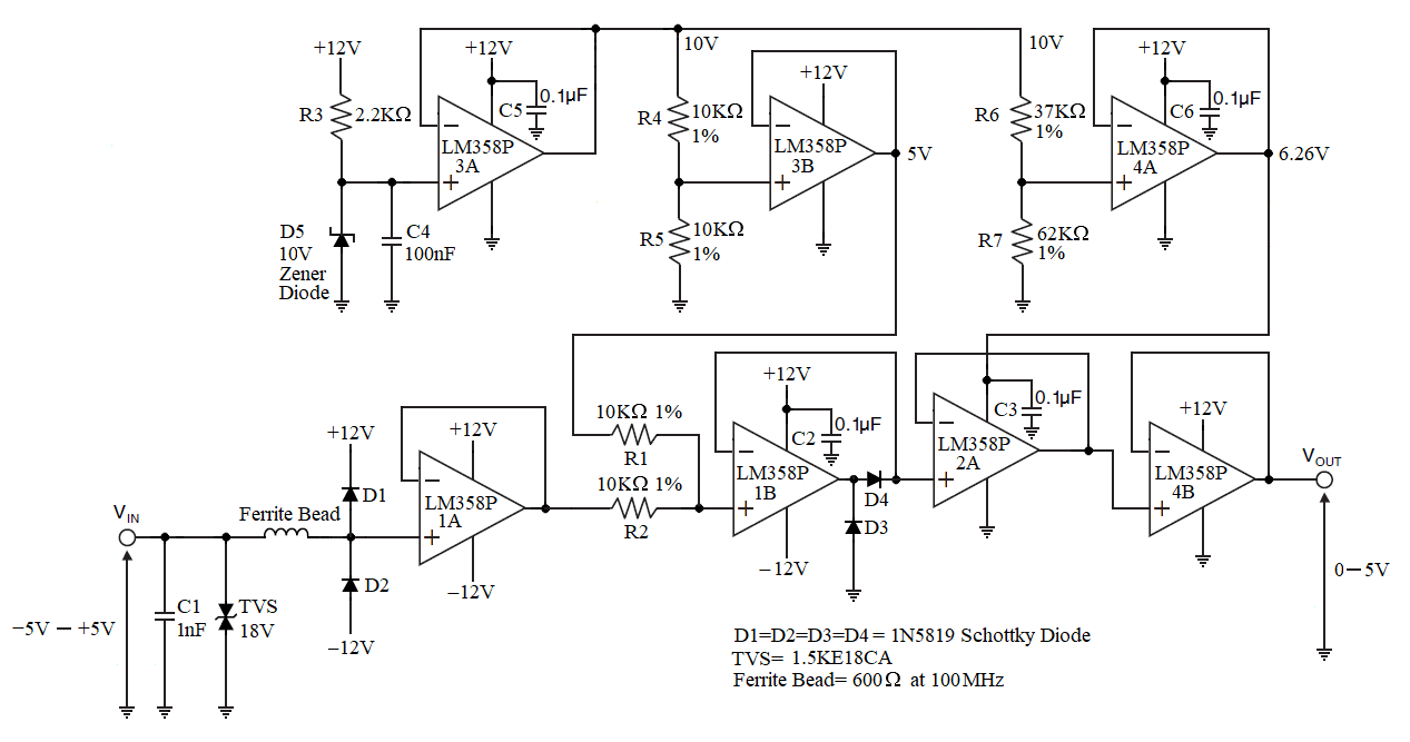
Analogue Input Module 2
Figure 5 shows the schematic diagram of the analogue input module 2 of the -5V to 5V to 0-5V signal converter, used with the ADC input of a 5V microcontroller. Its connections are shown in Figure 6.
As with the previous module, in this design we assumed that the input voltage range, VIN, is -12V to 12V. When -12V ≤ VIN < -5, VOUT = 0V. When -5V ≤ VIN ≤ +5V, VOUT = (VIN + 5V)/2. When 5.01V ≤ VIN ≤ 12V, VOUT will be a value from 5.01V to 5.07V, due to the electrical characteristics of the LM358P-2A used. The relationship between VOUT and VIN is shown in Figure 3.
Except for the buffer amplifier LM358P-4B from where the output voltage VOUT is obtained, the lower part the diagram is identical with that of the analogue module 1 of the -5V to +5V to 0-5V signal converter. The upper part obtains both the 5V and 6.26V reference voltages. R3, D5 (10V zener diode) and C4, together with the buffer amplifier LM358P-3A provide a 10V reference voltage from a 12V power supply. This 10V reference voltage is then divided by using resistors R4 and R5 to obtain a 5V reference voltage.
Next, the 5V reference voltage is connected to the non-inverting input of the buffer amplifier LM358P-3B, whose output is fixed as a 5V reference voltage capable of sourcing up to 20mA. Likewise, the 10V reference voltage is also divided by using R6 and R7 to obtain a 6.26V reference voltage. This 6.26V reference voltage is connected to the non-inverting input of the buffer amplifier LM358P-4A, whose output is fixed as a 6.26V reference voltage capable of sourcing up to 20mA.
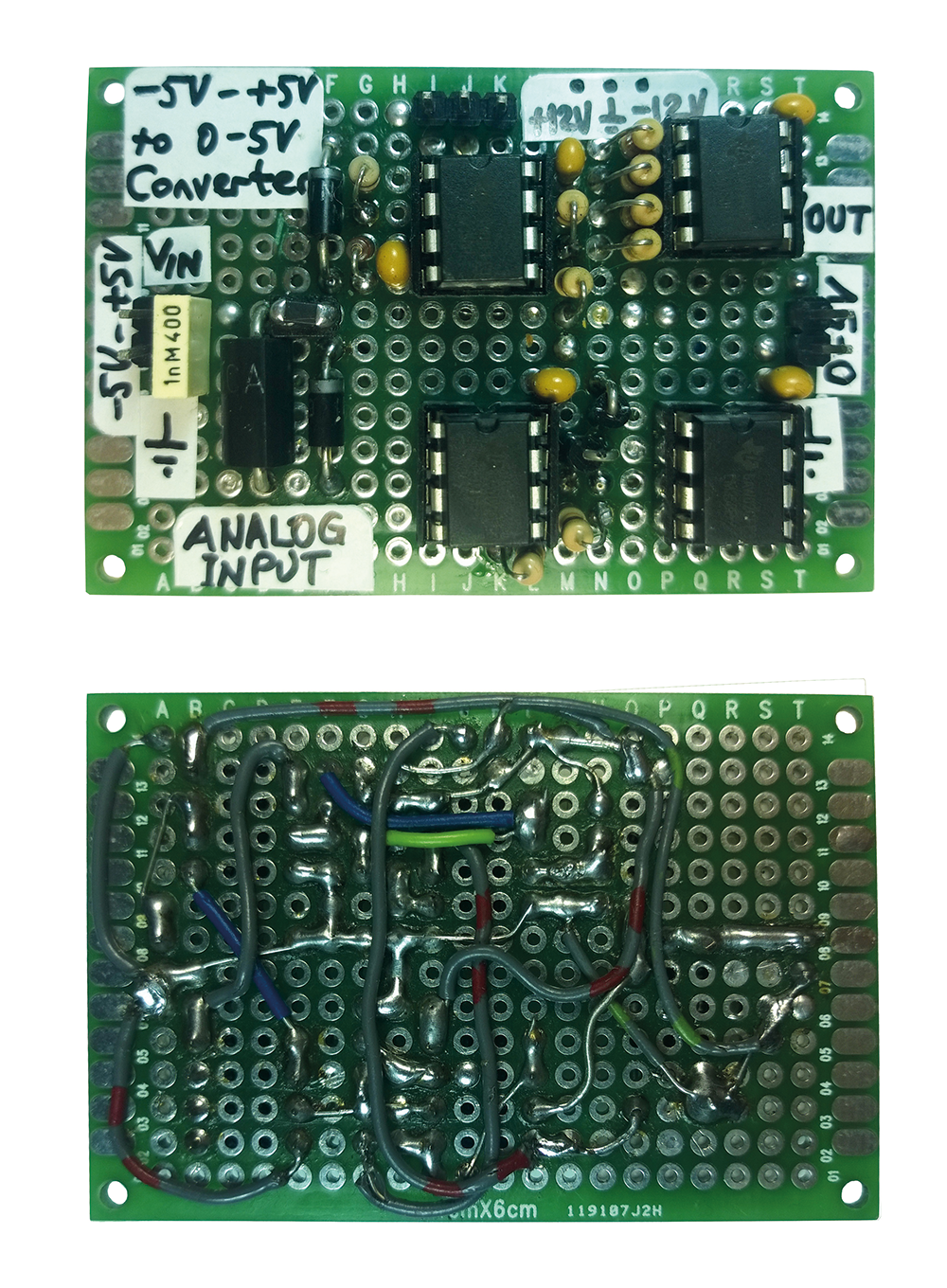
Table 1 provides some example input and output voltages. The top and bottom of this module’s prototype circuit are shown in Figure 7.
For proper operation make sure that R1 = R2, R4 = R5 and R7/(R6 + R7) = 62.62%.