The growing volumes of silicon ingots, wafers, integrated circuits (ICs), MEMS and other electronic packages requires equipment that performs non-destructive imaging and materials analysis. In addition, the continuously evolving high-volume production processes are rapidly migrating beyond industry standards. New device designs, packaging methods, shrinking dimensions, bonded wafer interfaces and increased product yields are driving a market for improved production equipment.
Challenges include higher levels of automation integration for component handling, improved cleanroom performance requirements, and scanning of ever-smaller components and interface connections. These conditions all advance scanning acoustic microscopy (SAM) technology, rapidly establishing it as a method of choice.
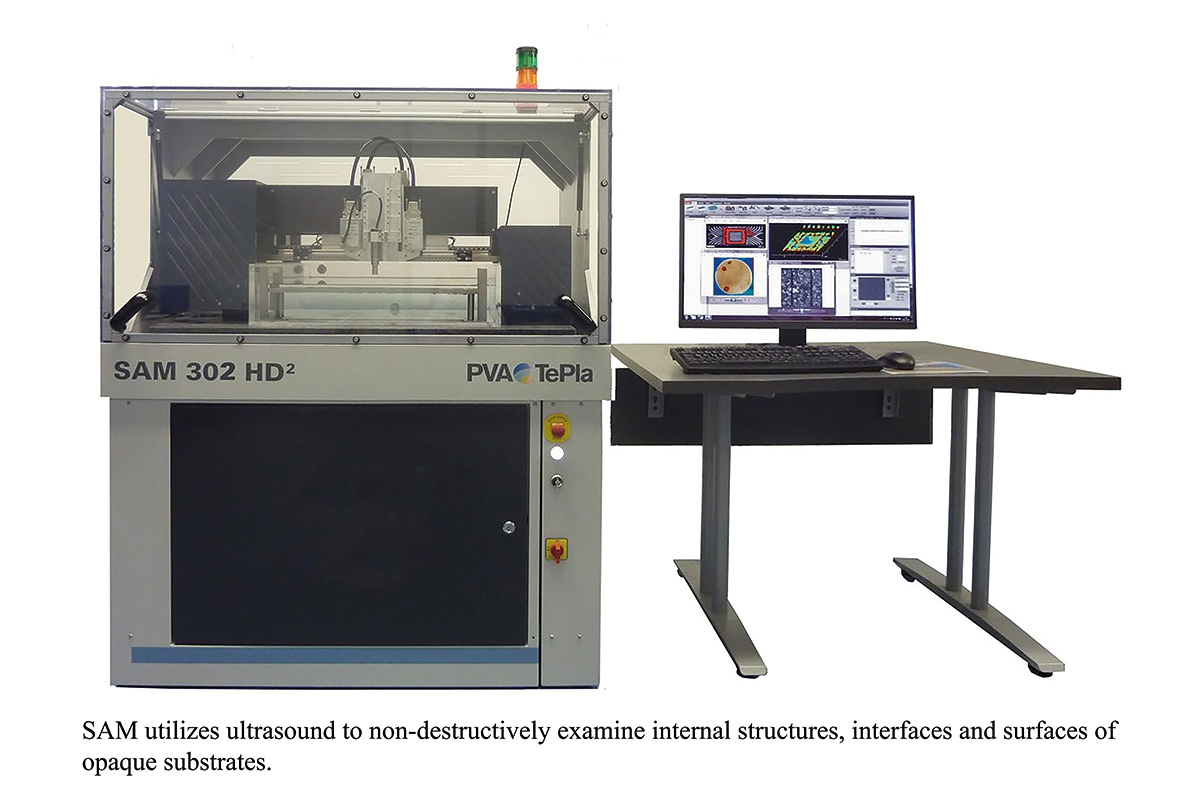
SAM Technology
SAM uses ultrasound waves to non-destructively examine internal structures, interfaces and surfaces of opaque substrates. It works by directing focused sound from a transducer at a small point on a target object. The sound hitting the object is either scattered, absorbed, reflected (scattered at 180°) or transmitted (scattered at 0°). By detecting the direction of scattered pulses and the ‘time of flight’, the presence of a boundary or object can be determined along with its distance.
A unique characteristic of acoustic microscopy is its ability to image the interaction of acoustic waves with the elastic properties of a specimen, allowing imaging the interior of an opaque material. To produce an image, samples are scanned point by point and line by line. Scanning modes range from single-layer views to tray scans and cross-sections. Multi-layer scans can include up to 50 independent layers. The resulting acoustic signatures can be put together into three-dimensional images that are analysed to detect and characterise device flaws such as cracks, delamination, inclusions and voids in bonding interfaces, and to evaluate soldering and other interface connections.
“Using ultrasound provides a clear advantage in ensuring good adhesion and mechanical integrity of devices,” said Peter Hoffrogge, Product Manager of PVA TePla Analytical Systems, a company that designs and manufactures advanced scanning acoustic microscopes. Compared to alternative techniques like X-ray, used to evaluate volumes and densities, ultrasound looks at interfaces, says Hoffrogge. “In an example of a sintered connection on a power device, the gaps are only a few nanometers,” he said. “With X-ray there’s no contrast, so you can’t tell whether the die has adhesion through the interlay or not. With ultrasound, it is easy to see.”
The challenge today is to perform this inspection at extremely high throughput with 100% accuracy in identifying and removing components that don’t meet the quality requirements. Often, these defects can occur in different layers of the device, calling for advanced equipment that can simultaneously inspect several layers and scanning multiple samples in handling trays in an automated way to accelerate the process.
However, as with other inspection systems, increased throughput requirements traditionally have required sacrificing image resolution. Fortunately, said Hoffrogge, today’s advanced inspection equipment can overcome these limitations. Much of it is custom designed to be integrated into other high-volume manufacturing systems, such as those inspecting crystal ingots, wafers and electronics packages in a range of standard sizes. For items with more unique product geometries or sizes, equipment can be semi-customised to meet the requirements of an application based on established, common components.
Pre-Developed, Integrated Systems
Today, SAM equipment exists that specifically handles standardised items such as bonded wafer inspection of MEMS, CMOS imaging sensors, and others. The equipment tests for inclusions or delaminated areas in the bonding interfaces and other defects.
“Typically, damage inspection is performed in a late stage of production to make sure the device is error-free, 100% flawless. This is typically done before dicing,” says Hoffrogge.
A bonded wafer inspection tool can be optimised for high throughput with four transducers and automated wafer handling. Cassette-loading systems are quick (open load port, SMIF, FOUP or customised input and output cassettes) for robots handling 5-12inch wafers and integrated scanners for wafer tracking, along with other features required of such systems.
For volume inspection of single-crystal ingots (e.g. Si, Ge, GaAs) a multiple-transducer scanning system (four heads) is used to estimate the 3D location of defects inside the crystal, so the tool can analyse voids and inclusions, estimating their depth and size. The tool can inspect 5-12inch Si ingots up to 400mm thickness and 75kg weight. Defect resolution may approach 100μm voids in silicon.
Hoffrogge says there are many systems in production, performing inline inspection of sensitive electronic devices transported in JEDEC trays. Regardless of the type of component inspected, each system includes integrated data analysis and automation software, GEM/SECS interface for fab-host communication and other key features.
Specific Equipment
When even higher throughput is required, multiple transducers can be used on a single substrate, with the images then stitched together, or multiple transducers can simultaneously scan multiple substrates.
Throughput can also be increased by incorporating ultra-fast single- or dual-gantry scanning systems or 6-axis robots. Other possible add-ons include axis-rotation (flipping), vacuum chucks and customised water tanks.
Hoffrogge suggests working with a company with a large portfolio of core, standard components to use or modify for a rapid and specific inspection solution. Having the complete value chain available from one vendor can speed the development process from the start through to complete process qualification, providing maximum value.
Even transducers, at the heart of all SAM systems, can be custom-manufactured to meet specific scanning requirements. Transducers can be adapted to each application or specific customer device and inspection requirement, ensuring the highest level of defect detection.
Some companies design and manufacture transducers in a very wide frequency range, from 3-2000MHz. They perform this work in-house, utilising proprietary thin-film technology developed over many years.
“It is possible to manufacture transducers within the standard cost and lead times of the industry,” said Hoffrogge. “Having all the equipment for manufacturing and testing in-house, eliminates the need to rely on third parties for items such as optical components, where there are often very significant lead times.”