By Tom Gregory, Future Facilities
Once seen as the ‘light source of the future’, LEDs are rapidly becoming the norm within a huge array of consumer and industrial electronics products. The design of LEDs however is a complex, multidisciplinary problem, with thermal optimisation and design proving a particular challenge.
Thermal Design Challenges
More than most “traditional” lighting technologies, LEDs are highly efficient, largely due to the direct conversion of electrical current to optical radiation in the semiconductor. Despite being significantly more efficient than incandescent or fluorescent lighting, however, a high amount of electrical power in LEDs is still converted to heat rather than light – and the higher the current, the more heat is created. This heat must be conducted away from the LEDs, because the semiconductor material is limited to a maximum temperature, and its characteristic properties, such as forward voltage, wavelength and lifetime, may vary with temperature. The result is that LEDs can appear drastically different depending on the temperature.
As temperature increases, the light output of LEDs can decrease by as much as 10%; similarly, maintaining the desired light colour is also heavily temperature-dependent. In addition to the light itself, changes in temperature can also impact reliability, with the expected operating life of LED lamps, usually between 25,000 and 50,000 hours, dropping considerably if the temperature isn’t managed effectively.
The end application can also radically alter how bright or colourful an LED is. With LEDs now being used in so many different environments, it is harder than ever for designers to guarantee their products will be used in a thermally-stable environment. Take the automotive industry as an example. In many automotive applications, devices need to operate at ambient temperatures to 85ºC. This means that manufacturers must build their devices to meet customer requirements for output, colour and operating life with the temperature in mind and allow for any temperature-induced performance shift.
Ultimately, only adequate thermal management can facilitate the full exploitation of LED performance and efficiency during operation. Proper cooling – of both the LED itself and the aluminium electrolytic capacitors employed in driver circuits – is central to the design process.
These fundamental challenges have been further added to by growing market demand for compact fixtures and lamps. Increasingly, smaller lighting fixtures are required in portable applications, such as entertainment lighting, so that they can be transported and handled more easily and are less obtrusive in use.
In retrofit applications, such as street lamps and domestic downlights, designers need to keep shapes and sizes within the limits defined by existing fixtures. This normally means squeezing the electronic driver circuit inside the fixture, and, in the case of directional lighting, the LED emitter module and lenses, too. This means that the heat must be dissipated from an ever-decreasing amount of space.
Thermal Management
For designers, the aim of thermal management is to transfer the heat generated by the device into the ambient air to prevent components overheating. The scope and complexity of thermal management depends on the amount of heat, the size of the source and the anticipated ambient conditions. Dealing with all of these factors requires a clearly-defined heat transfer path.
Typically, the system heat transfer path begins at the heat source (semiconductor junction layer), and travels via the PCB, heat sink and housing before finally reaching the ambient air; see Figure 1. The challenge lies in managing this heat transfer within the constraints of the power class and application of a device.
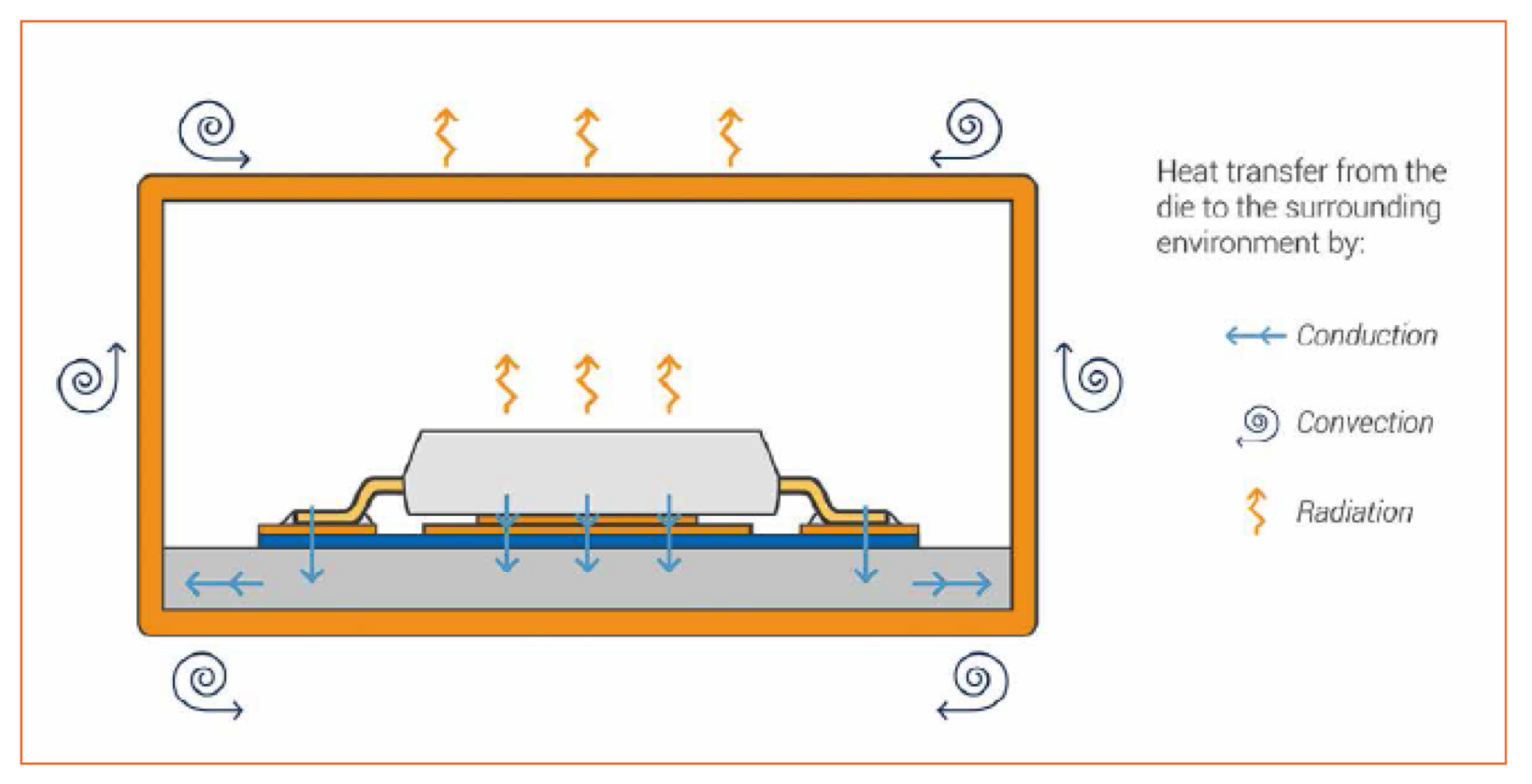
Figure 1: Heat transfer in an LED system
As a rule, the thermal management of an LED system can be broken down into three system levels: the LED itself, the sub-mount/PCB and the cooling unit. The heat path for system heat transfer can be described in the same terms. The heat generated in the LED barrier layer is transmitted through the LED housing (package) via the soldered joint and on to the PCB. At PCB level, the heat can be transported to the heat sink, and is often enhanced by specialist PCB construction. From the cooling unit (e.g. heat sink, system housing), the heat is finally transferred to the ambient environment through natural convection and thermal radiation. At each stage, designers are faced with a number of crucial decisions in order to optimise that heat transfer.
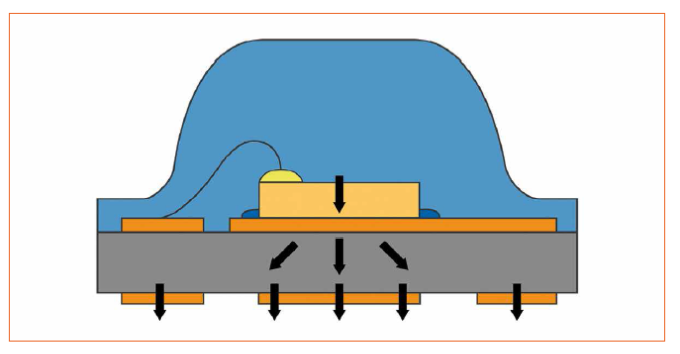
At the LED level, the type of housing has a significant impact on thermal management. To take a couple of examples, lead-frame-based LED housings and ceramic-based LED housings offer different approaches to heat transfer for designers.
In the case of a lead-frame-based housing (Figure 2), the semiconductor chip is mounted on a lead frame that, in most cases, consists of a plated copper alloy. The connection can be glued or soldered. Starting from the barrier layer, the heat is primarily dissipated from the package via the chip and lead frame. The amount of heat transfer that takes place via the bond wire is insignificant.

Figure 2: Heat conduction via lead(s)
In the case of LED packages based on ceramic substrates (Figure 3), the semiconductor chip is attached to the metallisation layer of the ceramic. The good thermal conductivity of the ceramics enables heat spreading in conjunction with the metallisation layer. The heat produced in the semiconductor is distributed via the metallisation layer and ceramic base material and transmitted to the PCB via the solder pad.

Figure 3: Heat conduction via ceramic substrate
Knowledge of the heat conduction path in the LED housing is important, as it enables the correct choice of subsequent system components (PCB, solder pads, etc.).
The thermal design of the PCB presents designers with another range of decisions; see Figure 4. Heat can be transferred over the PCB (horizontal conduction) or through the PCB (vertical conduction).
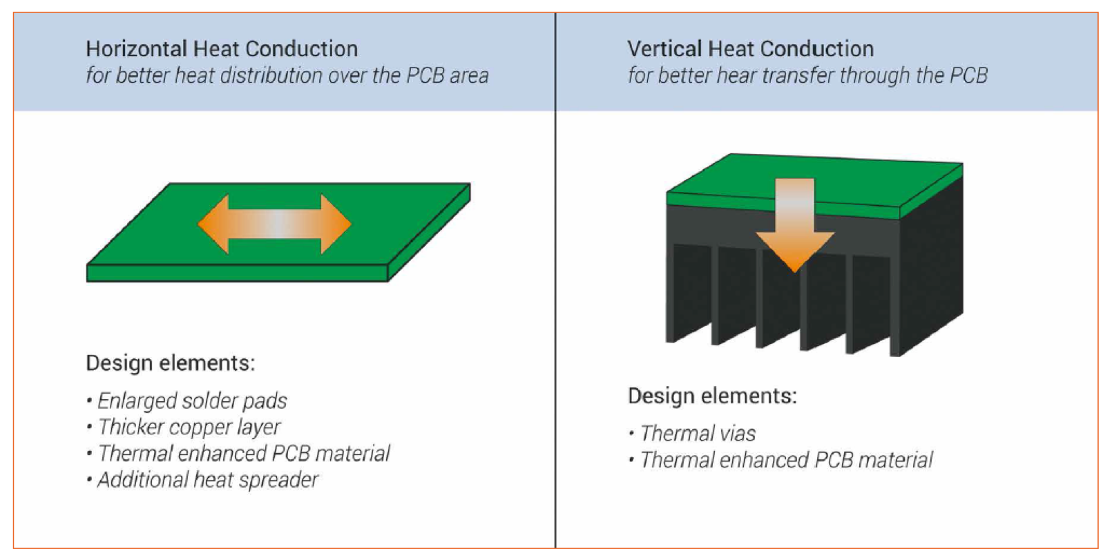
Figure 4: Illustration of horizontal vs vertical heat conduction
In both cases, conduction paths are impacted by a range of factors: the location of the LEDs on the PCB, to what level thermal losses need to be dissipated, and whether there are other potential heat sources nearby. Moreover, shrinking LED devices adds further complications. Smaller devices have a reduced contact area with the board; previously, older and larger packages meant that more heat spreading could be done on the device itself. Increasingly, these smaller devices are forcing this process to take place on the PCB instead.
These factors then impact material selection, the surface area required, the required thickness of the conducting layers and the need for thermal vias in the PCB design.
The final system layer is the point of transition to the ambient environment. From this point, heat can only be dissipated effectively via convection or radiation due to the low conductivity of air.
Most LED designs rely on natural rather than forced convection. This means designers require heat sinks that provide maximum surface area rather than using active methods like fans, or more sophisticated methods such as Peltier elements, heat pipes or water cooling.
Five Steps to LED Thermal
Simulation
Faced with all
these challenges, LED designers use thermal simulation to predict the
temperature of LED modules and to ensure their operation at the desired
conditions. Here is a typical example of how a design engineer could create a
thermal simulation of a LED bulb:
Step 1: Import and define materials
Import a fully-detailed model of the LED bulb. This can be imported using the STEP, IGES or STL CAD file formats.
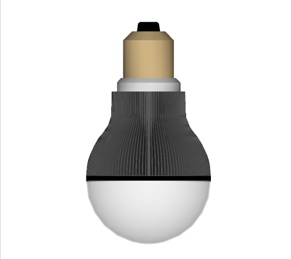
Figure 5: A typical CAD model of an LED bulb
Then, specify the material on each of the parts of the LED assembly. 6SigmaET
contains a library of material that can be used. If specialised materials are
used new material can be specified from data in the material datasheet.
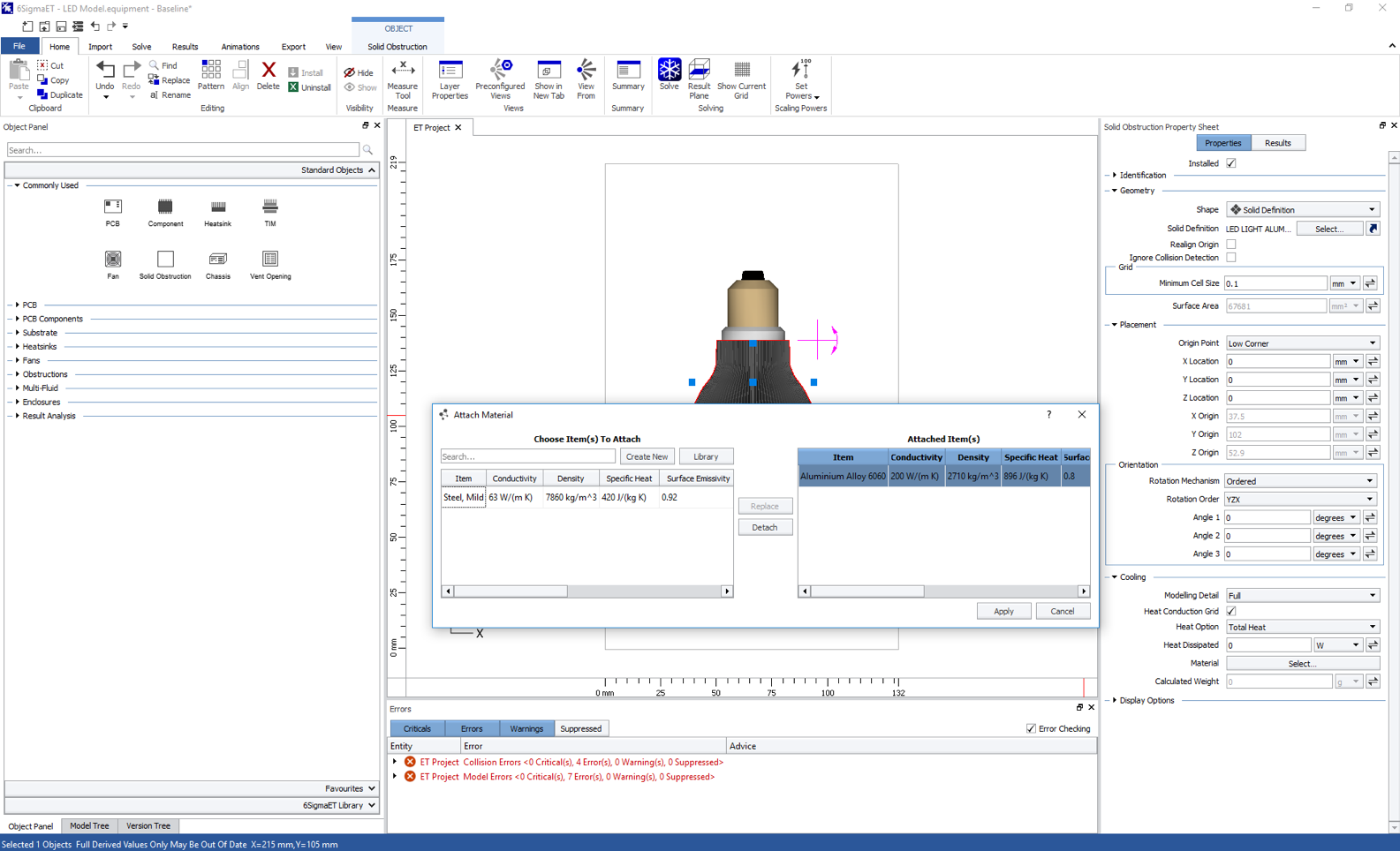
Figure 6: Defining the material properties of the design in 6SigmaET
Step 2: Add the printed circuit boards
The printed circuit boards in the light bulb, LED module board and a power board need to be included. Thermal simulation software can allow the import of PCB design from ECAD software using file formats including IDF, Gerber and ODB++. It is important to model the material used in the PCBs whether it is an aluminium, ceramic or FR4 core.
Step 3: Model the LED packages
Manufacturers of LED packages and modules typically provide thermal models of their products for use in thermal simulation. Use these thermal models to ensure the heat transfer from the LED package to the board is predicted accurately.
Increasingly, brands such as 6SigmaET are also encouraging the use of completely neutral file formats for the exchange of thermal models, allowing designers to import models created in a range of simulation software.
It is also essential to correctly set the power dissipation of the LEDs based on their expected operating conditions.
Step 4: Define the environment
It’s important to consider how the LED bulb is mounted since this will significantly impact how its heat is dissipated. In most thermal simulation tools, you can change the angle of gravity, which is an efficient and quick way of changing the orientation of the bulb without having to change the geometry.
Define the temperature of the environment to be the maximum possible temperature the bulb is designed to operate in.
Step 5: Run your simulation
Having built the LED model, it’s time to run the first CFD (Computational Fluid Dynamics) simulation. Don’t expect this to be a ‘right first time’ process, however. The whole point of running thermal simulations is that they can be tweaked and re-run multiple times in order to maximise the efficiency of the design, without the need to create numerous physical prototypes.
Dedicated Tools
As well as reducing the reliance on physical testing, the use of dedicated thermal simulation software offers other benefits, including a reduction of design risk and a 10-30% improvement in cooling for LED products. Overall, the use of simulation is estimated to save anything from a few weeks to several months in terms of total time to market for clients.
And it’s not just time that will be saved. According to estimates from Future Facilities, a CFD software and services company, by avoiding potential design failures, the use of thermal simulation software can save manufacturers upwards of £32,000 per year in unnecessary costs.
Given these potential costs and the unique array of challenges involved in the LED design process, thermal management – and by extension thermal simulation – will have an increasingly vital role to play in the future of LED design. By running simulations early on in the design process and ensuring that they have the right tools in place, LED manufacturers, designers and engineers can develop longer-lasting, more-reliable LED in shorter timeframes and at lower costs.